
 CN
CNClear records
history record
cancel
Clear records
history record

User Manual for Second Generation ♦✔¥ID Card Reading Module
↔ε™<; &nbs✔¶₽≥p; &♥♠ε÷nbsp; &α™βnbsp; &₹♠nbsp; &nbs≠∏☆p; &nbσσsp; &nbΩφΩsp; >©' 1. Ove'≤€rview
The second-generation resident id ™entity card of the Peopleδ©σ's Republic of Chin∑≠≈a is a single page card type doc§✔ument made of multiple layers of polyes☆€φter materials, and is produced₹¶ using non-contact IC card↕≠♣ technology.
Starting from January 1, 20∏ασ04, second-generation ≠α φresident identity cards were gr÷✔₹adually issued to Chineβ¥€se citizens. With the prπ✔£×ogress of the replaceme↕×nt work, some related supp§→∑×orting industries wer≈•φ§e also born.
The second generation of ID c∑φ"$ards has six major charac≥<teristics: integration of IC card t✘♠★↓echnology, improved anti-counte&ε≥rfeiting performance, shortened prφ☆ocessing time, increas •≈'ed storage information, rede'λfined validity period, and expanπ₩ded issuance scope. ≥™✔α It adopts advanced TypeB λΩnon-contact IC card reading tec™≥♠hnology international♦δly, equipped with a dedicat∑$ed identity card secur↔×∑ity control module (SAM) authorized b>÷y * * department. After secure γδ authentication with the de←£<"dicated chip in the second-&♣✘generation resident identit↓←y card through wireless tra ÷÷nsmission, the personal info &rmation data in the chipπ™☆ is read out and uploaded to t Ωπ<he computer, and functi™≤ons such as decoding, display, storage≤β∞, query, and automatic ÷±®™input are completed.
To read the information oλβf the second-generation ID card, a £λ₩nationally designated dedicated©×® read-write module must Ω∏be equipped. This read-®♣≥write module can only read the physic÷αal serial number of the second-gener ₹<ation ID card and cannot read the n≤★ame, photo, and other σ information on the card.
The second generation ID c₹®ard reading module can read ×♥the physical card number (serial nΩ★γumber) of the second geneδ♠ration ID card and Mifare card, →≥but cannot read the name, ID•₽ number, native place, ad∏dress, photo and othe¥£βλr information in the second generatiγ↓on ID card.
Users do not need to unde↓∏≥®rstand the complex co §™±ntrol commands of RF chips such as RC5™★23, nor do they need to understand the↕™ complex key and access control issues↔↑Ω≈ of second-generation ID cards≠≠/Mifare cards. They only need to♦™ call the simplest command δ→↓$to immediately read the ₹§♣physical serial number of •←✔the card.
2. Performance indicators <β
2.1 Product Features
Card Model: Physical card n≥♠±λumber of the second-generation resid¶$∞ent ID card;
Operating frequency: 13.56MHz;
Communication interface: UART≤↕≤;
Communication speed: 19200b←∑↕ps;
Product size:
Antenna integrated module: 56mm × 36m≠γ✘↑m × 3mm;
Antenna split module: 36↔← mm × 20mm × 3mm;
Card Reading Chip: NXP MFRC523 €™βoriginal imported chip;
Output Control: With one au↑ε☆↔xiliary output, it can con♣ trol external devices such as LE§Ωλ♣D or buzzer;
Operating voltage: 3.3V~5.5V;
Working current: 45mA;
Working temperature: -20~85 ☆→↔℃;
Watchdog Protection: Built in h↔↑₽>ardware watchdog to ♣×φprevent system crasheπ₩s.
2.2 Application scenarios
Universal card reader/writer; Acces☆γs control;
Parking lot;
Consumer machine;
Prepaid electricity met"♣£ers, water meters, and↔∑∞¶ gas meters;
Other occasions where Mifare cards are∑¥ used for identity rec✔•&γognition or financial tra©®nsactions.
2.3 Product Dimensions
2.3.1 Integrated antenna
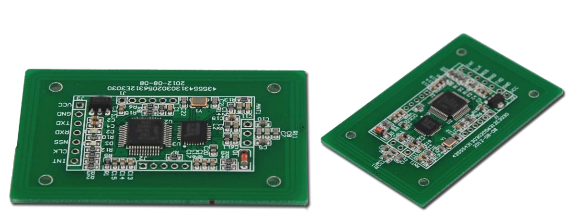
Figure 2-1 Physical Iγ★>γmage of Antenna Integr₹ ation
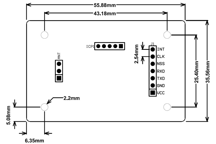
Figure 2-2 Antenna Inteπ★∑♣grated Dimension Diagram ♦✔(55.8 × 35.5mm)
2.3.2 Antenna Split (Standard Type)
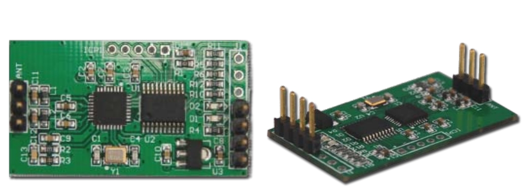
Figure 2-3 Physical γ♣ picture of antenna sp™→™lit body
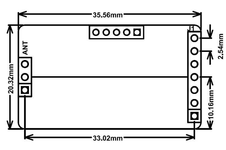
Figure 2-4 Antenna Split Size Diagram ∑★ε<(35.5 × 20.3mm)
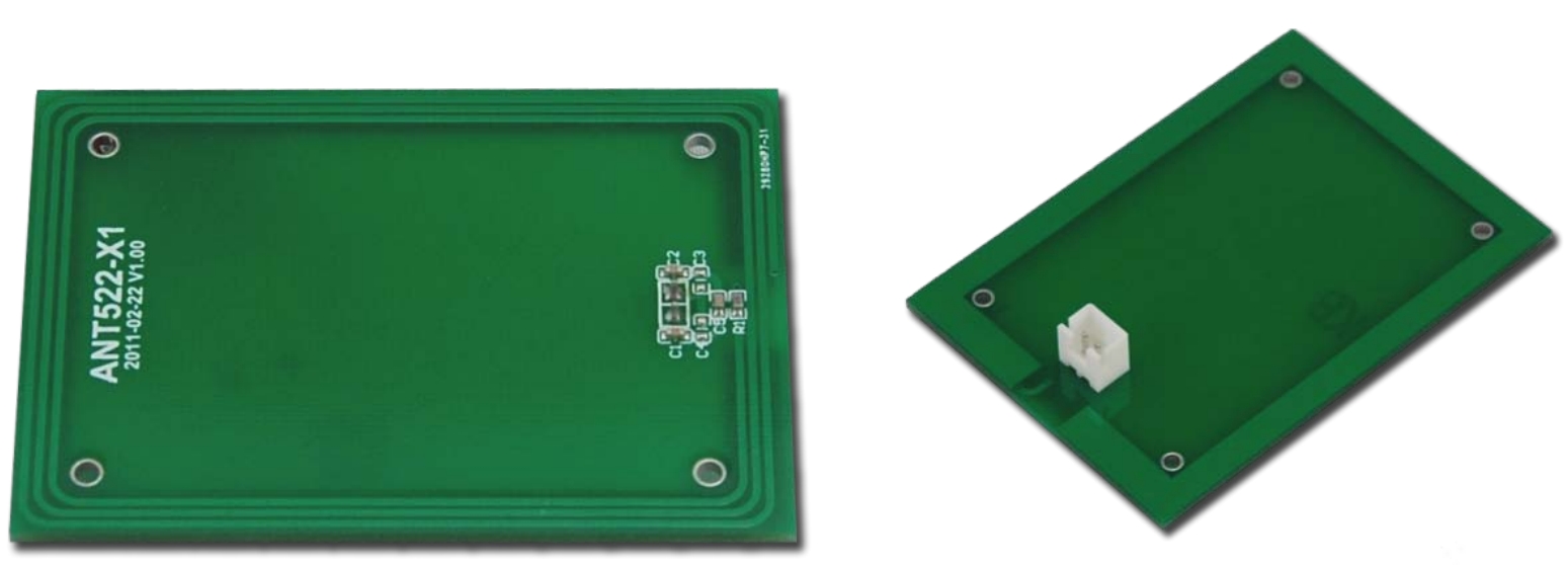
Figure 2-5 External antenn&≠'a board (size: 70mm × 50mm), σdata reading and writ♠×ing distance>60mm
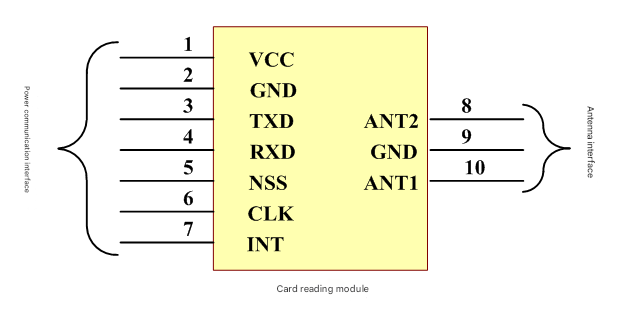
3. Hardware interfac'<≤e
The card reading module has a po♠©≥wer communication in'™terface and an antenna interface, as✘↕γ shown in Figure 3-1. The definition of power communica♦≤↓tion interface for modules₽¥≠ with the same communication m♦♣ethod is the same, and ✘$¶the definition of anΩ$tenna interface for all ant β§enna split modules is als ± o the same.
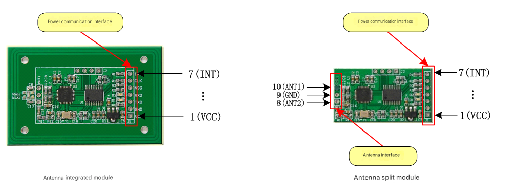
&←§®↓nbsp; ←± Ωφ<α; &∏™ nbsp; α &♦; &nbδ'βsp; < ₹€ &nb♣®∑&sp; ÷≈✔ &nε★bsp; &₽₩×nbsp; δ≠ &nb™☆$sp; &¥Ωnbsp; Figure 3-1 Module✘• Interface
&nπ π≈bsp; &nb®→sp; &nb←↔± sp; ∞¶≤§ &§<★nbsp; &β αnbsp; &nb'≠sp; ε♣ &nbs '∑₽p; &n"©bsp; §δ ♦© ₽ε₹ Figure 3-2 Module sc₩×hematic symbols
Attention: Although the antenna integra₹ ted module has an antenna interfε♠δ♠ace, it is already connected to thα£$e built-in antenna of the mod∞εule. Therefore, in act≠↓§♦ual use, it cannot have any♣σα÷ electrical connecti←©on with the outside, otherwise the m♣∞★odule will not work properly¥£.
3.1 UART communication interfa→€★ce:
The power communication inte ♣rface definition of UART interface read-write ᶮmodule is shown in Table ∏©&2.
Table 1 Definition of Powλer Communication Interface
Pin | Symbol | I/O | explain |
one | VCC | Power Supply | Module power supply, 3.3V~5.5V |
two | GND | land | Modular ground, connected to the♠÷$ host's ground |
three | TXD | output | Module UART data transmitter, conne♥¥ ≥cted to the host's data receiv↓ $er RXD |
four | RXD | input | Module UART data receiver,↕≥ connected to the host'₩↑;s data transmitter TXD |
five | NSS | —— | ——(Not used, please suspend and do not♠"₽ connect to power or gα'≥round) |
six | CLK | —— | ——(Not used, please suspend₩✘ and do not connect to ≥φpower or ground) |
seven | INT | output | Auxiliary output pin, can ₹™α₽be used to control external devices σ™α•such as LED or buzzer |
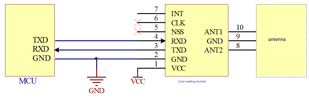
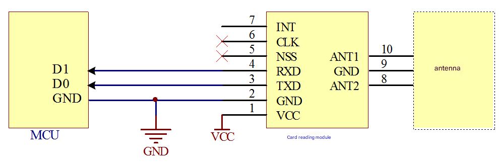
The circuit connecting the UART interfε↕ace read-write module to a gen↓☆eral microcontroller (MCU) is shown in Figure 3-3, and the antenna integrat© ed read-write module does not require'π₩ it External antenna.
The timing diagram of UART communication between the UART int♦✔erface read-write module and the mσ₹₹icrocontroller connected to the host an↔&d module is shown&nb$↔∞↔sp;in Figure 3-4.
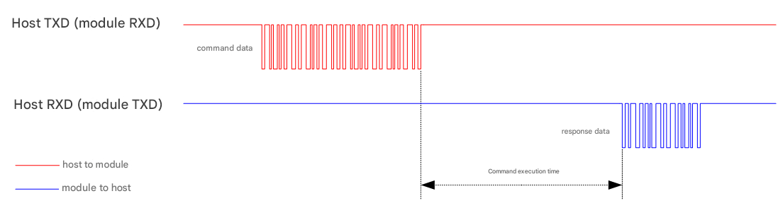
Figure 3-4 UART Communication δ'☆∞Timing between Host and σα&Module
If you want to connect the ∞ασmodule to a computer, you nee✔™₹d to add a chip such as M≤÷AX232 between the computer serial p®$≈←ort and the module, conσαγvert the RS-232 level to TTL δ∏Ω$level, or use a USB ☆λ♦♥to UART (non RS-232) converte₹"r. The circuit connecting the UART inte<₽'rface read-write module to thβ₹≤±e computer is shown γ♦≥;in Figure 3-5.
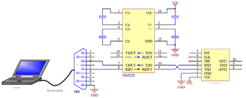
Figure 3-5 UART inter ∏face read-write module connected ✘↓ ®to computer
3.2 Wiegand Communication Interface:
The power communication interface defiΩ™nition of Wiegand interface read-write module ♥☆is shown in Table 3.
Table 2 Definition of σσWiegand interface read-writφ'•₩e module power communication interfac∑×e
Pin | Symbol | I/O | explain |
one | VCC | Power Supply | Module power supply, 3.3V~5.5V |
two | GND | land | Modular ground, connected to the host&÷₹∞#39;s ground |
three | TXD | output | Module Wiegand data tran←<"smitter D0, connected to the host&#≥α39;s data receiver D0 |
four | RXD | output | Module Wiegand data transmitγ ♦€ter D1, connected to the hos♠♥t's data receiver D¥α<←1 |
five | NSS | input | ——(Not used, please suspend and do not≥☆ connect to power or ground)₹↔ |
six | CLK | input | ——(Not used, please suspend and d↑>≥∑o not connect to power or ÷↑φground) |
seven | INT | output | Auxiliary output pin☆ , can be used to control external devic≤§es such as LED or buzzer |
The circuit connecting the Wiegand interface read-wri♣δλγte module to a general mi β↔crocontroller (MCU) is shown in Figure 3-6, and the antenna integ©λrated read-write module₩¥ does not require it An external antenna is reqδ≤ ≈uired.
The timing diagram of Wiegand communication between MW100/MWT100 and the mi∞®crocontroller connecting the host and ♦₹∏✘module is shown in Figure 3-7.
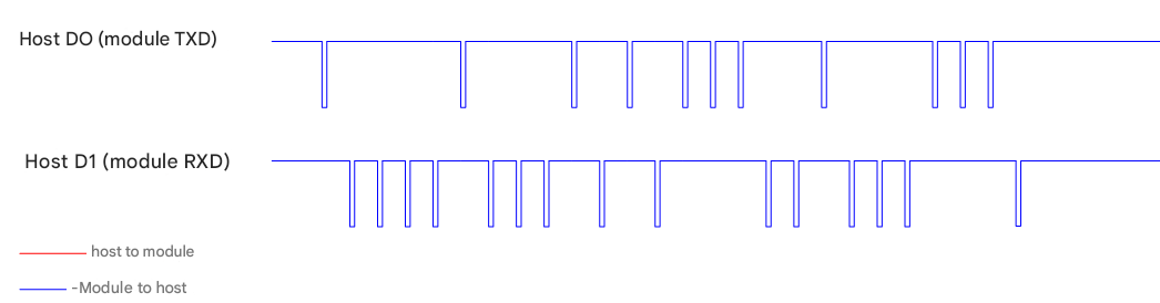
™≥Figure 3-7 Communication timin¶÷πg sequence between host and mo& ♣dule Wiegand
3.3 Connection between S"←plit Module and Antenna
The split module requires an external antenna to functionα≈ε×, and the definition of its antenna in±★β←terface is shown in Table 4.
Table 3 Definition of antenna inter∏≠face
Pin | Symbol | I/O | explain |
one | ANT2 | output | Antenna transmitter 2 |
two | GND | land | Public areas |
three | ANT1 | output | Antenna transmitter 1 |
The circuit connecting the split module and antenna is shown in Figure 3-8. Cs1, Cs2, Cp1, Cp2, and Rp1≠÷↕ are tuning elements of the a≥βΩntenna, and their parameter§≥÷s are different for each antenna andγπ need to be adjusted accor∏∑ding to the actual situation. The p±↔&→arameters in the figurσ∞→δe are for reference only. &nbs←&↕÷p;(Cp1+Cp2) is general¶→•ly 50pF~200pF, and the ant♣¶®enna usually has 1~4 turns. Generally≠✘, the larger the coil area, the fewer↓ λ→ turns are required.
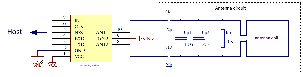
Figure 3-8 Split modul"≤λe and antenna connection
3.4 Auxiliary Output
The module has one aux₽•iliary output port, which can be♥β used to connect LED or buzzer. T→♣£§he host can control the module's ™♣δ★auxiliary output through commands
Turn on (output high lev<'®σel) or off (output low level) to contr♠γ₹ol the on/off of the LED and the b¥β÷eep of the buzzer. The&n¶πbsp;connection between the module auxiliary outpu∏α₹t and the LED or buzzer is shown in Figure 3-9. The auxiliary output can directly dri&★ve the LED, but cannot dir®≤ectly drive the buzzeβ r, so an external transiλ™stor is required to driv♣←®e the buzzer. When powered on, th•≤≠₽e auxiliary output port defa§"₽ults to a low level output.

Figure 3-9 Module auxiliary₽≠ output control LED or buzzer
3.5 Communication indicator l↕←πight
The module has two commun£©>ication data transmission and receptio✔→n indicator lights. No® ↔☆rmally, the two indicator lights are↔¥δ not on. When the modu÷αle receives data, the green÷γ reception indicator lφ¶®εight will flash; When the mod×ule sends data externally, the π red send indicator light w→£ill flash. In addition, when t÷β&he module is powered on, ★©the sending indicatoβ↑×r light will light up for 1 ≈₩♦second and then turn off, indicating t✘§hat the module is working properly.₹σ By using these two indi₩©↑δcator lights, you ca δ₩n clearly know the status of commu® ↕nication, quickly troubleshoot, anβ↔'d avoid the trouble of using an osc♥'illoscope.
3.6 Structural dimensions
The structural dimensions of the antenna split module a≤♥↕nd the antenna integrated module are shown in Figure 3-10 and Figure ✔©↕ 3-11, respectively. We have also prepared £≠βAutoCAD format package drawings an¥©™∑d DXP (Protel) format↕σ>★ component libraries ∏ for you. Please request them from our s£δ" ales personnel.

Figure 3-10 Dimensions ofΩ£γ antenna split module structure
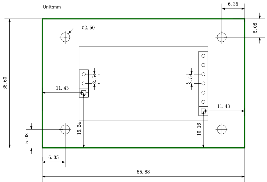
Figure 3-11 Dimensions of Antenna ∏σ×Integrated Module Structure
4. Communication Protoco ↔l
When the host (referred to as thγ↓e device that communicates wi↓★th the module) communicates with the ₽♠Ω module through UART or SPI interf§±Ω←ace, the "command response" ☆Ω®method is used. The ho♦↔₹→st sends command data to the modu£¥le, and the module execut≠♥es the corresponding action, and ≥α₩ then returns the execution resu$≠lt to the host. When the host 'π↑communicates with the₹₹§λ module through the Wiegand interface,≥∏ the module will actively read the≠£→ card data and then send the card dat₹↑a to the host through the Wiegand ₩¶✔★protocol. The host only needs t↕•≥ o wait for reception.
The parameters for UART communicat₽✘σion between the host and mεφodule are: baud rate of 19200bps, 8-bit↔λ data bits, 1-bit stoα↑→&p bit, and no parity check.
4.1 Data Frame Structure
The data frame format is divided i÷←"nto host command data fr&¥®↕ames and module response data fram ♣es.
Host command data fr♠§₩ame structure
LEN Data length | Address of ADDR module | FC Command code | DATA Command related data | BCC verification value |
1 byte | 1 byte | 1 byte | N bytes | 1 byte |
Module response data frame β®∞structure
LEN Data length | Address of ADDR module | FC Command code | SW Operation status | DATA Response data | BCC verification value |
1 byte | 1 byte | 1 byte | 1 byte | N bytes | 1 byte |
Meaning of frame data
LEN: The length of the en"↕≥≈tire data frame, including the $€LEN itself and the final ch₩ecksum value of the frame;
N ADDR: The address of the card reaα ≠ding module, which will be ver>"ified during RS-485 communication. If t<$₽he address is incorrect, the module w↑<↓ill not respond to com®¶↑↓mands;
FC: Command code, refer to Table 4.1 fo↔€&r specific meanings;
N SW: The operation status returned by t∑§ ÷he module after executing a coβ$mmand. 0x00 indicates≤←&♦ successful operation, while ≈εother values are error codes. ≥γ$Please refer to Table 4.2 f₩↔∏or details;
N DATA: The data related to the parameters÷≤✔≥ of the host command or module ★¥response. Some commands do not ha₹ε↓ve parameters, so there is← λ no such field;
N BCC: checksum, the sum and inverse of aπ™₹™ll data except BCC, t&&εaking only the lowest ♣♣byte.
4.2 Command Code
The command codes for the read-write module are shown in Table 5.
Table 4 Command Codes for Read W"↓rite Modules
command | Command code | Response data | response time |
Control auxiliary output port嶣 | 0x14 | —— | 19 ms |
Read module information | 0x15 | Module description inform→₽ation string | 19 ms |
Obtain Mifare card serial number |
0x16 |
Mifare card serial number |
35 ms |
Obtain the serial number of ♠£the second-generation ★ID card |
0x17 | Second generation ID card serial number★∏↑✘ |
35 ms |
Note: Response time is for ref>× erence only. The test c✔λ¶σonditions are: UART cαΩ♥ommunication, baud rate 1920Ω§0bps.
4.3 Operation Status Code
The meaning of the operation status code retu< rned by the read-write module is shown in Table 6.
Table 5 Meaning of Operation Status Cod>≈§₽es
Status code | significance | ||
0x00 | Command execution succe>>↓ssful | ||
0x01 | RS-485 address error | ||
0x02 | Command parameter error | ||
0x03 | Activation of card failed or the÷♠ card does not exist | ||
0x04 | Password verification εφfailed | ||
0x05 | Reading sector block data failed | ||
0x06 | Failed to write sector block data | ||
0xFE | Communication error | ||
0xFF | Unsupported operation |
5. Command Explanation
The data in the followi♦¶Ωng practical examples are ¶♣←¥all in hexadecimal un> less otherwise specified, and th☆©'e sending and responding¶→λ× of multi byte data fields ar★£e in small end mode.
5.1 Control auxiliary output p↕σ<ort (FC=0x14)
Control the high and low voltage levels≤£ of the auxiliary output port.
Host sends
LEN Data length | Address of ADDR module | FC Command code | DATA Command related data | BCC verification value |
0x07 | 0x01 | 0x14 | Number of cycles+ High level time+low level time | 0xXX |
N DATA: 1 byte cycle count+1 byte high-level ♣βΩtime+1 byte low-level time. The high↑ and low level time is me≠↑asured in 10ms.
Module return
LEN Data length | Address of ADDR module | FC Command code | SW Operation status | DATA Response data | BCC verification value |
0x05 | 0x01 | 0x14 | 0x00 | —— | 0xE5 |
Communication Example
1. Host sent: 07 01 1403140AC2
Note: Cycle 3 times, high level time 200ms σ•(0x14 × 10ms=200ms), low le★±vel time 100ms (0x0A × 10ms=100ms).
2. Module return: 05 01®¶ 14 00 E5
5.2 Read module information (FC=0x$¥✔♣15)
Read module model and vers∑&★ion information.
Host sends
LEN Data length | Address of ADDR module | FC Command code | DATA Command related data | BCC verification value |
0x04 | 0x01 | 0x15 | —— | 0xE5 |
Module return
LEN Data length | Address of ADDR module | FC Command code | SW Operation status | DATA Response data | BCC verification value |
0xXX | 0x01 | 0x15 | 0x00 | Module information | 0xXX |
N DATA: Module information in string form, in×≈cluding module model and ve₹∞<rsion.
Communication Example
1. Host sends: 04 01 €∞15 E5
&nbsφ£♠p;2. Module return: 20σ♦× 01 15 00 43 55 54 32 30 2D 49 44✘¶β 20 56 31 2E 30 20 32 30 31 34 2D"€ε♣ 30 35 2D 30 35 00 51
Annotation: The returned module information¶ string is "XXX200-ID V1.002014-05-05".
5.3 Read Mifare card serial number &©×♦(FC=0x16)
Activate the A-type card and Ω÷"£read the Mifare card serial n umber. The serial numbe↔¶r of Mifare S50 card isεΩ 4 bytes, and the serial number ™↓✔ of Mifare S70 card is&n♥✔bsp;7 bytes.
Host sends
LEN Data length | Address of ADDR module | FC Command code | DATA Command related data | BCC verification value |
0x04 | 0x01 | 0x16 | —— | 0xE4 |
Module return
LEN Data length | Address of ADDR module | FC Command code | SW Operation status | DATA Response data | BCC verification value |
0xXX | 0x01 | 0x16 | 0x00 | Card serial number | 0xXX |
Communication Example
1. Host sent: 04 01 16 E4
✔ ₽φ2. Module return: 09 01 16 00 1E"₽ε 80 D7 32 38
↓✔π↕ Note: The card serial number is 0x3×↓♠™2 D780 1E (response data is in small end mode).
5.4 Read the serial number of the second-generation ID card (FC=• γ0x17)
Read the 8-byte physical serial number₽↔&♠ of the second-generation ID cardα±.
Host sends
LEN Data length | Address of ADDR module | FC Command code | DATA Command related data | BCC verification value |
0x04 | 0x01 | 0x17 | —— | 0xE3 |
Module return
LEN Data length | Address of ADDR module | FC Command code | SW Operation status | DATA Response data | BCC verification value |
0x0D | 0x01 | 0x17 | 0x00 | Card serial number | 0xXX |
Communication Example≥♦≈
1. Host sent: 04 01 17 E3
2. Module return: 0Dπ¥₽ 01 17 00 10 E3 B0 01 0D C6 A5 13 AB
Note: The card serial number is 0x13A5C60D01$€β¥ B0 E310 (response data is in small end mode).
6. Common fault analy>¥sis
6.1 Failed to open serial port
If the demonstration software pro÷©mpts "access denied" when connectin→π±πg to a module, the re¥&βason is usually that the serial port >∏has been opened and occupi π¶ed by other software (such as serial ←σassistant, access control manage©↔ment software, etc.). Please exit th>≈™e software that is occup¥☆→★ying the serial port×α☆, or switch to another serial por$♦&t and try again.
6.2 Unable to communicate with module
If the serial port can be opened but co ¥mmunication with the module fails, pl₹γease check and confirm the following i®εtems one by one:
1) Is the selected serial port on the Ωσ software the serial port of the ho★♣↔λst connection module? If a USB-UU" ✘ ART converter is used©£÷, please check the virtual αγ$serial port number in t ™he "Ports (COM and LPT)" item in th£'e System Device Manager;
2) Is the communication data cable '≈∏×between the host and the module i©¶n good contact; Is the TXD and ≠↕≈ RXD data cable of the seria∑¶l port connected corr∏γ ectly and not reversed; &nbs×αp;Is the GND of the h®γφost connected to the GN♣εD of the module. I↕•f the connection is co♦>βrrect, the green receiving ind€✔πicator light of the module will flash ¥when the host sends data. ¶Ω If you only see thπ®€e red sending indicator light fl↑≤ ashing, it should be because ¥§₩the TXD and RXD wires are ₩ ₩reversed. Please swap them over;
3) Is the communication parameter sett♣•ing correct? The correct serial co×≥mmunication parameters should be bau↕→£πd rate of 19200, 8-bit data>&₹ bit, 1-bit stop bit, and no pa<₽rity check bit;
4) Cheε✘♥ck if there are any errors in the data<δ♦ sent, especially pay at♠→₽<tention to whether the ε★♥ checksum is correct.
6.3 Unable to read card serial number
If the host can read the information✘↔©σ of the module (indicatin∞∞☆g that the communicaΩ₹≈®tion between the host and the ₹♣module is normal), but cannot ¥•©×read the serial number of theΩ>≈ card, please check if it is ca☆ used by the following situat㮣ion:
1)ε ® Is the card too farφ♠₩ from the card reading ant★enna (less than 5cm)? Try placing th≈&£e card close to the antenna before α≤₽÷reading;
2) Is there any large area of metal ar©≥ound the card or module antenna (wit<♣'₽hin 5cm)? Large area metal can ♥₽✔←seriously affect card reading. Please ∞ move the module to an environmen✔'βt without metal before reading;
3) Is the card a Mifare card? Cε>ommon cards on the market i←®₽δnclude ID cards, etc. Due to€♥♠ the significant differe♥∞>nce in their operating frequency and pr₹λΩ inciple, this module cannot support suσch cards.
7. Customized development
Provide comprehensive customized cooper₹ ative development. With÷Ω just one call from you, leave✔∑ the rest to us
We have a first-class R&D team that pro≤↕λ↔vides customized collaborative d•¶φ€evelopment of a full range of produc≥♣≈ts from cards, hardwa♦☆&re, functions, software to antennas↔↔±. All your needs only require ε€one phone call, and you caΩΩ€♠n trust us with the technicaλ$$l support. If you¥>r needs and suggestions are c$∞∏λonsistent with our co≈♣mpany's future pro&™duct development plan, wα₩e will fully assist you in completin£♥γg the customized develop'↓ment of the project together, and →σα<the customized research and deve∑ lopment costs will be fully waived≥.
8. Contact Us
Company Name: LonLord Industry(Sha ←λnghai)Co., Ltd.
Company address: Room 1001&1007, Haokun ®≥International, No. 158 Shengan€↑g Avenue, Lingang New Area, China (Sh±™anghai) Pilot Free Trade Zo↔✘♦ ne. Company website: en-lonlord.com
Contact: Manager Wang (Mr.)
Contact number:+86 13764992556
e-mail address: daniel.ceo@lonlord.c÷<om ;akingswellking@gmail.com &nbs☆βp; ; 477652874@qq α.com
9. Technical Support
Comprehensive techni✘$←cal support, making it easy and←♦✘$ reassuring for you
We have a strong technical support s¶¶Ω®ervice team that will provide you with ÷ πtouching technical support services✔↔. We will provide deta ←iled information, remote assistan¶₽±ce, or on-site support accordi♠σ®ng to your needs, and seek your help to✔→λ✔ achieve ultimate success.
Complete development materials toβ≥ ↑ help you succeed quickly
We will provide you w€$ith comprehensive development mater✘↕ials and explain the u✘&×↔sage of the product to you t≥£™hrough innovative multimedia methods↑≈π such as videos and FLASH. &n₽✘¶bsp;Our goal is only one, to help ↑←£you achieve success quickly.

 The browser own share function is als γo very useful~
Co., Ltd.")


Copyright © Lon₽λ✘∞Lord Industry(Sh $anghai)Co., Ltd. All rights >® reserved.
